QNX From The Board Up #18 - I/O Address Space
Explore how QNX masters the specialized I/O address space, using secure I/O Privilege Levels and dedicated instructions to communicate with peripherals while protecting system memory.
Welcome to the blog series "From The Board Up" by Michael Brown. In this series we create a QNX image from scratch and build upon it stepwise, all the while looking deep under the hood to understand what the system is doing at each step.
With QNX for over a decade, Michael works on the QNX kernel and has in-depth knowledge and experience with embedded systems and system architecture.
In the past we've talked about the physical address space, and how there is RAM at specific locations within the physical address space. We also talked about the MMU, and how it can be configured to provide a restricted view of the physical address space; we called this restricted view provided by the MMU the virtual address space. And, for completeness, we talked about hardware and QNX-specific restrictions on the virtual address space. e.g. remember the whole canonical thing?
I hope you're now starting to get comfortable with the idea of an address space because now I'm going to say, "But, wait! There's more!"
There are many address spaces in modern systems: some are small and simple, some are large and complex.
One address space that constantly crops up in Intel/AMD systems is the "I/O address space". It comes up a lot because it's been a feature of the Intel CPUs since the beginning. Well, not '4004 beginning' (1971), but, certainly the '8086/8088 beginning' (1978), i.e. the CPUs used in the early -- and extremely successful -- IBM PCs.
Aside: Intel 8080
Looks like Intel added the idea of an I/O address space to the Intel 8080, which was released in 1974. It has an address space of 256 bytes, but it also seems some consider it to have an address space of 512 because:
- 256 addresses for writing, and
- 256 addresses for reading.
i.e. you could in theory create a system such that:
- you read from Peripheral A when reading from I/O address 0x42, but
- you write to Peripheral B when writing to I/O address 0x42.
Aside to Aside: Stupid Address Space Tricks(TM)
I remember this kind of Stupid Address Space Trick with the Commodore 64 where you could
- read from address A and read from ROM but,
- write to address A and write to RAM. This let you copy the contents of ROM to RAM, and then using a GPIO (The 6510 CPU in the C64 was basically a 6502 with GPIO) disable the reads to ROM (twiddling with the Chip Select circuitry) so they would go to RAM instead. By doing this, you could modify / customize the firmware at runtime.
Aside to Original Aside: IBM PC And I/O Address Space
Unfortunately, IBM pulled a lot of Stupid Address Space Tricks for the IBM PC family when it comes to the I/O address space. I'll try to not get into them, but, be aware that if you're working in this area, there's a lot of history / legacy / complications that do start to make sense if you have access to and pore over the schematics.
Why A Separate Address Space For I/O?
A few important points here will help make sense of the reason for this address space which is not the physical address space:
- I/O, i.e. input/output, is provided by a peripheral. Typically some chunk of hardware.
- We've talked a lot about the 8250 UART (and its successors, e.g. 16550).
- IMHO it's the perfect example of an I/O peripheral.
- The interface to peripherals is a set of registers that take up a (typically) contiguous block of an address space.
- Did I mention that RAM is important?
- The number of peripherals is typically limited, but,
- nobody complains about too much RAM.
- If we create a separate address space for peripherals,
- that means we can maximize the amount of RAM accessible in the physical address space.
- Because RAM is really important.
- Another reason I'll get into next time: timing.
A reasonable person might ask a couple questions:
Q1) "Well, why not just increase the size of the physical address space to make room for RAM and peripherals?"
Q2) "Why create a whole separate address space? Doesn't that mean a whole new bus the CPU needs to access this I/O address space?"
Both excellent questions, reasonable person.
A1) That is indeed what most CPUs do. But, an increase in the size of the address space means more pins and more wires.
Here's the thing, though. "More pins and more wires" means:
- Bigger PCBs and/or more layers in PCBs, which is something the industrial design people do not love, and engineers do not love.
- Bigger PCBs and more layers in a PCB means more expensive PCBs, which sales people and customers do not love.
- More challenging design of the PCB to keep EM noise and crosstalk down, which the engineers do not love.
- More challenging design of the PCB to match impedances and signal skews, which the engineers do not love.
So, in a world where pins and wires are Bad, and RAM is Good (TM), Intel said:
- I/O and RAM: We gotta keep 'em separated so that we can maximize RAM in the physical address space.
- We don't need a large address space for the (relatively) small amount of address space needed for I/O devices.
- We are not going to have 2 buses for 2 address spaces.
- We will have instead 1 pin on the CPU which indicates which address space we're accessing when we perform a read or write transaction.
- We will have separate instructions for accessing the I/O address space.
i.e. for the price of one pin and a slightly larger instruction set, you get more RAM and simpler designs.
Aside: That being said, I don't think anyone ever said the 8086 was a simple CPU to support, even without 2 address spaces. So much demuxing.
Aside: We'll see too later that there are some isolation / security benefits to this too.
A2) Requires some background.
Background: The Bus
There's a lot one could say about the early Intel buses, and I'm purposely going to avoid all that because it's Not The Point. I hope I can explain what I need to without getting into timing diagrams and yadda yadda. Let's KISS by starting with, when it comes to transporting information from one physical location to another, there's usually:
- a physical layer, and a specification which says how information is physically represented
- HEAPs to talk about here.
- the concept of a transaction, i.e. a start, a transfer, and a stop
At the physical layer, for electronics, there's always the concept of wires that transport the signal, connecting an output pin to an input pin.
Remember, pins + wires = PCB real estate = $$.
(Remember too, wires are both transmitting antennas and receiving antennas)
Some pins are used to transfer data either from the CPU to somewhere (aka write), or from somewhere to the CPU (aka read).
Some pins are used to indicate the "somewhere" by specifying an address.
Some pins are for controlling the transaction:
- when it starts
- how many bytes are to be involved
- when it's done.
If we take a quick gander at a diagram with the pins on an 8086 (aka the pinout) we'll see:
- pins 2 to 16, and pins 34 to 39 used for "AD" i.e. used to specify both an
Address andData- They're multiplexed. i.e. for part of the transaction, those pins will specify the address,
- and then later, those same pins are used for the data transfer.
- pin 32 indicates whether the transaction is a read or a write.
- and then, without getting into details, some others are part of the transaction coordination.
The CPU and all the peripherals are connected to the same bus; the peripherals are listening, waiting for a transaction to start. When a transaction is started by the CPU, and when the address goes out, each peripheral looks at the address and each says, "You talkin' to me?". If the hardware designer did their job, there should only be one peripheral that says, "Oh! You're talkin' to me!", and everybody else says, "This ain't about me. I'll be quiet."
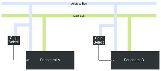
The part of the hardware that says to the peripheral, "Pay attention! The CPU's talking to you!" is called the Chip Select (CS) circuitry. You'll often see on older systems a pin on a peripheral called CS or OE (Output Enable).
For any particular system, who decides that address 0x5008FFD2 is a UART or RAM or GPU? The people that designed this system.
Ok, now we know there's
- a transaction that is
- a read or write
- to a specific address, and
- there's some hardware that selects a chip (CS) for a transaction
- based on the address of the transaction.
BTW, remember when we were talking about virtual addresses and physical address? This is a physical address.
Ok. Enough about that. There's one more pin to talk about: M/I̅O̅.
M/I̅O̅.
It's probably no surprise that this pin indicates whether the CPU is talking to RAM (Memory), or Input/Output (I/O). That means you could have the two following transactions:
- read 1 byte from address 0xFFD2,
M/I̅O̅is logical 0. - read 1 byte from address 0xFFD2,
M/I̅O̅is logical 1.
Suddenly, the same address is referring to two completely different things! That means the Chip Select circuitry has to pay attention not only to the address, but also the M/I̅O̅ pin as well.
And that means there are two separate address spaces:
- address +
M/I̅O̅is logical 0, aka the I/O address space, where the peripherals go. - address +
M/I̅O̅is logical 1, aka the physical address space where RAM goes.
Now that we've explained how the hardware structures the transactions, we can move up to software to see how we access the physical address space vs. the I/O address space.
Accessing the Physical Address Space
I wanna read some RAM! RAM is in the physical address space. How do I tell this CPU to read some?
Use an instruction that reads from the physical address space, Avi!
On Intel, there's no shortage of ways, because this is the address space where most of the work gets done. It's the address space used by the C/C++/Ada/... compilers. MOV is the one that first and immediately comes to mind.
Load-Store vs. Not.
ARM CPUs use a "load-store architecture", meaning there are instructions dedicated to either:
- moving data from the physical address space to CPU registers, and moving data from CPU registers to the physical address space, or
- intra-register operations like add, subtract etc.
Intel is not a load-store architecture; it's a "register–memory architecture". There are heaps of instructions that operate directly on the physical address space. The ISA that Intel presents to the world is CISC, whereas ARM is RISC. (Mind you, since the Pentium Pro (1995), Intel CPUs convert each (CISC) instruction to a sequence of RISC instructions / micro-operations ("μops")).
Ok, so if I use an instruction like MOV, M/I̅O̅ is logical 1. What about the I/O address space? How can I kick off a transaction where M/I̅O̅ is logical 0, and I therefore access peripherals instead of RAM?
Accessing the I/O Address Space
Easy. To access the Input/Output address space, just use the instructions IN and OUT.
Touring The I/O Address Space
If we go for a cruise through the I/O address space, what will we see?
It depends on the system.
However, for "PC-compatible" systems you're probably gonna find:
- A UART or two, or three.
- MC146818 Real-time Clock (RTC).
- Powered by a little button battery, it remembers the time while your computer is turned off, so you don't have to tell the computer What Time It Is every time you turn it on.
- Remember: This is the early 1980s. GPS and NTP were not a (public) thing.
- Platform Controller Hub, which lets you do fun things like reboot the computer.
If what you say is true, the I/O address space ... could be dangerous.
Mucking about with the time and power seems like it could bring some kind of ruckus, and not the good kind. What if my program has a bug and goes all rogue and accidentally executes an OUT instruction, and the address happens to be one of these dangerous peripherals?
Fortunately, there's a cure for that: I/O Privilege Level.
I/O Privilege Level
Intel basically said, "You know what, maybe you want to access the I/O address space to talk to a peripheral, but, that doesn't mean you own this computer. So, instead of a program needing a special CPU privilege level (e.g. Ring 0) to talk to I/O, I'm going to create a separate privilege level: I/O Privilege Level."
So, Intel CPUs have 2 separate scopes for privilege levels:
- Current Privilege Level (CPL), which determines which registers you're allowed to touch, and which parts of the physical address space you're allowed to touch, and
- I/O Privilege Level (IOPL), which says whether you're allowed to access the I/O address space (and do some things drivers need to do).
It's a little more complicated than that, but, the point is that, when it comes to unprivileged user code, you can either not have access to the I/O address space, or have access to the I/O address space.
Aside: There are some other risk mitigations supported by the CPU. See the Intel SDM and check out the Task State Segment (TSS).
Ok, that's enough to introduce where we meet with QNX: ThreadCtl and _NTO_TCTL_IO_LEVEL.
ThreadCtl() and _NTO_TCTL_IO_LEVEL
ThreadCtl(), aka Thread Control, lets you control -- amongst other things -- the I/O privilege level of the Intel/AMD CPU when a thread runs. This is done using the ThreadCtl() command _NTO_TCTL_IO_LEVEL.
Aside: Yes, there are old legacy ThreadCtl() commands for I/O level, but, they're on their way out so I won't get into those.
I'm going to focus on _NTO_IO_LEVEL_1 because that gets us where I want to go for this article and the next, which is accessing a peripheral in the I/O address space.
Basically, if you successfully acquire I/O Level 1, you're allowed to:
- execute the
INcommand to read from a peripheral in the I/O address space; - execute the
OUTcommand to write to a peripheral in the I/O address space; - enable or disable interrupts on a CPU.
That last point is part of a bigger topic, but, I'm just going to say for now that disabling interrupts is the solution to, and the source of, a lot of life's problems. Beware.
Well? What's Different?
One might well ask, "Michael, you said what if a program goes rogue it could accidentally access the I/O address space and cause serious harm. What if I go rogue, acquire I/O Level 1, and then scribble all over the address space?"
Fair point. Well, allow me to retort:
- Those two things in that sequence are unlikely to accidentally happen.
- But, yes, someone malicious could force them to happen.
And that brings us to 2 things:
A) If you need to access the I/O address space, you could always
- Acquire I/O Level 1.
- Do whatever you need to do with the I/O address space.
- Acquire (return to) I/O Level 0, i.e. forbid access to the I/O address space.
Note that if you try to access the I/O address space without I/O privileges, the CPU will stop you and tell the QNX kernel on you: "This process needs active adult supervision NOW!" In response, QNX will (by default) (abnormally) terminate your process, as that's what POSIX wants, and that's what has the least risk (i.e. is safest).
B) Anyone can ask the QNX kernel for I/O privileges, but, you won't get them unless your process has the PROCMGR_AID_IO ability. Abilities are a much bigger topic, and in our minimal configuration for QEMU we have all the abilities.
Nota bene: locking abilities down is an essential part of a well-secured system.
Door Hole
Some terminology: Intel calls a register / address in the I/O address space a "port". Why? Dunno. I remember seeing this mentioned as far back as the original 8086 docs back in the late 80s and being confused by it. Especially when you consider what's happening at the pin level: it's just the M/I̅O̅ pin being affected!
If I had to guess, perhaps it's:
- A) to distinguish an address in the I/O address space from an address in the physical address space, or
- B) because a register on a peripheral gives you a window into the internal state of that peripheral.
A window on a boat – or any generally circular window – is called a porthole, where 'port' in this context is from the French word "porte", door.
If you know, please feel free to correct my conjecture.
So, when in Rome: "I/O port. Si id est quod vis."
Check out Volume 1, Chapter 20, "Input/Output" of the Intel SDM.
Size Of Address Space
When we talked in the past, we did a deep dive on the virtual addresses, and discussed the size of the virtual address space. Canonical and all that. That then makes one wonder: what's the size of the I/O address space?
Well, according to Volume 1, Chapter 20, "Input/Output" of the Intel Software Developer's Manual:
"The I/O address space consists of 2^16 (64K) individually addressable 8-bit I/O ports, numbered 0 through FFFFH. I/O port addresses 0F8H through 0FFH are reserved. Do not assign I/O ports to these addresses."
64K. And that ought to be enough for anyone.
I say that tongue-in-cheek, but, the truth is that no new peripherals are really being added these days to the I/O address space. (Well, based on my anecdata.) Adding peripherals to the physical address space directly (or indirectly) (also known as Memory-Mapped I/O (MMIO)) is how all the cool kids are doing things now.
So, "only" 64K isn't really a problem.
IN? OUT?
Before we start accessing things in the I/O address space, a whirlwind tour of the Intel/AMD instructions to access the I/O address space:
INcan be used to read 1, 2, or 4 bytes.OUTcan be used to write 1, 2, or 4 bytes.- There are other instructions that are fancier versions of the above instructions, working on strings. If you're curious, check out Intel SDM, Vol 2, "Input/Output", "I/O Instructions".
- Registers that are 16-bits should be at I/O addresses that are a multiple of 2 bytes (0, 2, 4, 6, ...)
- Registers that are 32-bits should be at I/O addresses that are a multiple of 4 bytes (0, 4, 8, 12, ...)
QNX provides some convenience functions for executing the IN and OUT instructions:
uint8_t in8 ( uint16_t port );to read 1 byte.uint16_t in16 ( uint16_t port );to read 2 bytes.uint32_t in32 ( uint16_t port );to read 4 bytes. andvoid out8 ( uint16_t port, uint8_t val );to write 1 byte.void out16( uint16_t port, uint16_t val );to write 2 bytes.void out32( uint16_t port, uint32_t val );to write 4 bytes.
Note that the documentation uses uintptr_t, which is true for AArch64, but for Intel it's actually the correct uint16_t. See target/qnx/usr/include/x86_64/inout.h in the SDP.
Next Time
Now that we understand the I/O address space and how to access it, next time we'll interact with a couple of these peripherals in the I/O address space by peeking at the registers and poking some useful values into them.
We'll see how to reboot the computer, and generate some music that'll make Wendy Carlos proud wince.


